I stumbled across an interesting post that led me to this site:
pshdl.org
It seems that there is an effort to create a new language that replaces/overlays traditional HDL such as Verilog and VHDL. The thought is that these languages originate pre-FPGA and have a lot of non-synthesizable concepts built into them. PSHDL may become a language that simplifies the general learning curve and process of realizing synthesizable designs. If you go to the root page of the link sited above, it will bring you to a webtool for generating equivalent, presumably, synthesizable HDL code.
Showing posts with label HDL. Show all posts
Showing posts with label HDL. Show all posts
Wednesday, January 22, 2014
Sunday, November 24, 2013
PWM VHDL Module
Here is yet another PWM (Pulse Width Modulation) module! What distinguishes this module from most other PWM modules is that it's parameterized. When dealing with LEDs this becomes a very useful feature since each type of LED responds differently (in terms of light) when presented with a PWM signal. This module will allow you to adjust the clock prescaler and the number of quantas. What does this mean you ask? Let me explain with the help of a simple picture...

Basically the PWM signal is produced via a multi-process module. The first process is a "prescaling process". This process takes the input clock and divides it down by the amount you specify. This process is not critical towards its operation and could be removed if you want to minimize your logic.
The next process is the "Accumulate process". This process is responsible for determining when to switch the PWM outputs logic state. Basically it takes the prescaler's divided clock and accumulates/increments a counter on each cycle. One time "quanta" is equivalent to one cycle of the PWM divided clock.
The final process is the "modulate" process. This is the key process to generating the PWM signal. It determines when to switch the PWM output signal based on the PWM accumulator and the PWM input signal. The accumulator continually counts up towards the maximum quanta value and then rolls over to 0 where the process continues to count. The PWM input determines when to bring the PWM output low. A larger PWM input means the PWM output will remain HI for a longer period of time which produces a brighter output on the LED (or dimmer depending on how the LED is connected). In order to maintain a constant level of illumination it is important to ensure that the refresh rate of the PWM cycle is above the human eye's flicker fusion rate. This is generally understood to be around 16Hz but you should target 60Hz or higher. The general criteria for these configurable parameters should satisfy the following equation:
Here is a demo of this module running on a Terasic DE0-NANO.
Download: PWM.vhd

The next process is the "Accumulate process". This process is responsible for determining when to switch the PWM outputs logic state. Basically it takes the prescaler's divided clock and accumulates/increments a counter on each cycle. One time "quanta" is equivalent to one cycle of the PWM divided clock.
The final process is the "modulate" process. This is the key process to generating the PWM signal. It determines when to switch the PWM output signal based on the PWM accumulator and the PWM input signal. The accumulator continually counts up towards the maximum quanta value and then rolls over to 0 where the process continues to count. The PWM input determines when to bring the PWM output low. A larger PWM input means the PWM output will remain HI for a longer period of time which produces a brighter output on the LED (or dimmer depending on how the LED is connected). In order to maintain a constant level of illumination it is important to ensure that the refresh rate of the PWM cycle is above the human eye's flicker fusion rate. This is generally understood to be around 16Hz but you should target 60Hz or higher. The general criteria for these configurable parameters should satisfy the following equation:
60<=(f_CLK/prescaler)/quantas
For instance, a 100MHz clock prescaled by 3125 with 128 time quantas yields a refresh rate of 250Hz which is well above the minimum and should be visually flicker-free.
Here is a demo of this module running on a Terasic DE0-NANO.
Download: PWM.vhd
Friday, January 27, 2012
FPGA to 74HC595 Shift Register Module in Verilog
I have had this 74HC595 IC sitting around for quite some time. And earlier this week I decided it was time for me to actually start using it...or at least start learning how I could use it. This chip is a Serial-In Parallel-Out 8-bit shift register that can be used in a variety of ways and it can be cascaded with more of these ICs to create a larger shift register if needed. My plan is to use this newly developed module to act as a low pin count interface between the FPGA and my 16x2 Character LCD module. This will allow me to utilize 4-wires to control the 8-bit parallel interface on the LCD (not including the LCD control lines). This reduced the FPGA pin utilization from 11 pins down to 7 pins...not to shabby. Anyways for those that are interested, the code is linked below. Please note: this module is very much application specific and that it does not enable all practical uses of the 74HC595 IC. For instance, the SRCLR signal is not used and is permanently tied to VCC so that it never clears the register; this of course, may not suit your needs, however the code is heavily commented and adaptation of the code should be fairly simple.
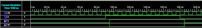
Simulation:
The functional operation of the module can be seen in this timing diagram simulation:

The yellow markers are showing the beginning and end of one complete 8-bit shift operation. This simulation is using a 50ns clock period which is slightly slower than the 24MHz clock that my actual FPGA is using. This simulation shows that it takes about 89 clocks to process a request. 89 clocks at 24MHz is about 3.7us.
Signal Descriptions:
Simulation:
The functional operation of the module can be seen in this timing diagram simulation:

Signal Descriptions:
- RDY: A bit that indicates that the FPGA_2_ShiftReg is idle and is ready to process a request
- RCLK: A signal sent to the shift register which instructs the output registers to read from the shift register taps
- SRCLK: A signal sent to the shift register which instructs the 8-bit shift register to shift the register bits and read from the serial input and push it into the LSB.
- OE: A signal sent to the shift register which sets the output in either Hi-Z (output disabled) or Lo-Z (output enabled). This is an active low signal.
- SER_OUT: The Serial signal sent to the shift register.
- CLK: The FPGA's local oscillator which drives the rest of the logic.
- BYTE_IN: An 8-bit value that is fed into the FPGA_2_ShiftReg module
- PB: A signal created for simulation purposes to instruct the module to read the 8-bit value from BYTE_IN. Every time this pushbutton is pressed the FPGA_2_ShiftReg module is activated and instructed to read the BYTE_IN. Also the driving module (the module that instantiates and uses the FPGA_2_ShiftReg module) increments the BYTE_IN value by one.
DOWNLOAD: FPGA_2_ShiftReg GitHub Repo
Wednesday, December 28, 2011
An implementation of a basic character LCD controller in Verilog
For a while now, I have been wanting to post my code that I developed during my GPS project using a FPGA board. Creating the LCD controller module was the meat of the project and I know many people are interested in how one might approach such a project. I have plans on providing a full-fledged tutorial on how I designed this module, but it is still in the works. In the meantime, I will provide you with the Verilog code which is fairly well commented and with a little cross correlation with the data sheet for the ST7066 the code should be for the most part, self-explanatory. Eventually this post will be edited with a more formal discussion of this code but for now we will have to make due with just the code.
Here is a screenshot of a simulation of what this module does after the initialization phase and you write the ascii value of "C" (0x43) as a data operation. The markers indicate the start and end of the module's execution of this operation.

Here is a screenshot of a simulation of what this module does after the initialization phase and you write the ascii value of "C" (0x43) as a data operation. The markers indicate the start and end of the module's execution of this operation.

DOWNLOAD: FPGA_2_LCD.v
Saturday, June 25, 2011
GPS to 16x2 Character LCD Using an FPGA
Note: The GPS coordinates shown will not lead you to me. The GPS module at the time of recording this, was not locked onto my coordinates...so don't try hunting me down..else you will find yourself in the Atlantic =P
Below is a basic block diagram that helps to illustrate what the FPGA does in the system. The FPGA has 3 modules: A Serial Module, a Parser Module, and an LCD Controller Module. The serial module is only responsible for acquiring the serial data at the specified baud rate. Over sampling is used in the FPGA to help minimize bit errors. The serial module passes the raw data to the parser module. At this point in time the raw data is the NMEA messages (with the overhead information removed, i.e. stopbit/startbit). The parser module waits for the occurrence of a '$' which indicates the start of an MTK/NMEA message. Once the '$' is received, the parser extracts the message type and checks for a "GGA" message. If the current message is a GGA message, then we extract the Latitude and Longitude based on the standard format of the GGA message. This is currently being done by counting the characters; however, counting the comma delimiters work just as well. The parser module passes the latitude and longitude data to the LCD module as it is received on the serial line. The LCD controller module handles the initialization process required to set the LCD module into an operative mode, and it handles all the timing and writing data to the display.

This is an on-going project and I plan to add many more features to it. Below are some changes that I plan on making in the future.
For those interested in knowing more about this project, or want more information about certain aspects of the HDL code that I wrote, please don't hesitate to post a comment.
For those interested in the LCD controller module's code, go here: LCD Controller.
Or to download all of the related HDL files, go here: GPS2LCD_Files.zip
My project was featured on Sparkfun's Main Page! Pretty cool and I got some good constructive criticism.
Future Improvements/Additions:
- Write the serial stream from the serial module to a Block Memory or RAM
- Read the data in a Block Memory or RAM and feed the data into the Parser Module.
- Perform mathematical operations on the acquired data, such as computing the displacement from the current location to the last saved location.
For those interested in the LCD controller module's code, go here: LCD Controller.
Or to download all of the related HDL files, go here: GPS2LCD_Files.zip
My project was featured on Sparkfun's Main Page! Pretty cool and I got some good constructive criticism.
Thursday, May 19, 2011
Using an MCP3002 ADC for Interfacing an FPGA with a Photocell
The MCP3002 ADC Chip is a very handy device. You can interface with it via a very simple SPI (Serial Peripheral Interface) protocol. The Verilog module that I designed to interface with this chip works beautifully.
The module I created uses both channels of the MCP3002 in an "interlaced" single-ended mode. The module is strictly configured to work with a local oscillator of 24MHz, but minor adjustments to the process that converts the local clock to a 1.2MHz clock is all that needs to be modified. The 1.2MHz clock is the maximum frequency that the IC can operate at while powered at 2.7V as specified in the datasheet (pg3) under the "Timing Parameters". In my case my FPGA uses 3.3V logic so Fclk(max) should reside somewhere between this and 3.2MHz. If we assume a linear relationship between voltage and operating frequency, then the maximum expected operating frequency at 3.3V would be ~1.688MHz, thus operating at 1.2MHz "should" be a safe level of operation while pushing the IC to work at its maximum.
As far as the code goes, it is really self explanatory. I would recommend anyone that is attempting to use this code to have a copy of the datasheet on hand so that you can see the relationship from my code and the datasheet's timing diagram. Figure 5-1 was specifically used to design this Verilog Module.
On a hardware interfacing note, be sure to pay attention to Figure 4-2 in the datasheet, this clearly states that the ADC's CH0 and CH1 input signals NEED to be buffered (i.e. use an opamp in a buffer configuration or similar). If you skip this, your maximum operating frequency will be lower that the one defined in the datasheet.
The code that I provide here is free to use however you would like, but I would appreciate it if you give me credit for my work. Also constructive criticism is welcome, if you see something that could be done better another way, let me know.
Download: MCP3002 ADC Module
The module I created uses both channels of the MCP3002 in an "interlaced" single-ended mode. The module is strictly configured to work with a local oscillator of 24MHz, but minor adjustments to the process that converts the local clock to a 1.2MHz clock is all that needs to be modified. The 1.2MHz clock is the maximum frequency that the IC can operate at while powered at 2.7V as specified in the datasheet (pg3) under the "Timing Parameters". In my case my FPGA uses 3.3V logic so Fclk(max) should reside somewhere between this and 3.2MHz. If we assume a linear relationship between voltage and operating frequency, then the maximum expected operating frequency at 3.3V would be ~1.688MHz, thus operating at 1.2MHz "should" be a safe level of operation while pushing the IC to work at its maximum.
As far as the code goes, it is really self explanatory. I would recommend anyone that is attempting to use this code to have a copy of the datasheet on hand so that you can see the relationship from my code and the datasheet's timing diagram. Figure 5-1 was specifically used to design this Verilog Module.
On a hardware interfacing note, be sure to pay attention to Figure 4-2 in the datasheet, this clearly states that the ADC's CH0 and CH1 input signals NEED to be buffered (i.e. use an opamp in a buffer configuration or similar). If you skip this, your maximum operating frequency will be lower that the one defined in the datasheet.
The code that I provide here is free to use however you would like, but I would appreciate it if you give me credit for my work. Also constructive criticism is welcome, if you see something that could be done better another way, let me know.
Wednesday, October 28, 2009
Update: Xilinx Simulation
With the recent official release of Windows 7, I decided to update my laptop to 64-bit Windows 7 instead of Vista 32-bit. The process was for the most part, completely painless. But by switching to a 64-bit OS an interesting problem (or more correctly, an annoyance) showed up when trying to simulate some HDL code I have been working on.
It turns out that Xilinx ISE does not have much support for 64-bit asside from generating bit files. When trying to simulate in ISE in 64-bit mode you will notice that you are limited to ModelSIM which I am not that familiar with, but I definiately didn't have much luck with it.
If you are looking to simulate some HDL in the 64-bit ISE, your best chances for success is to use the 32-bit ISE instead. Luckilly, Xilinx was nice and installed the 32-bit programs when you installed 64-bit ISE. Just go to your Program Files Xilinx Folder and locate the 32-bit ISE. It will launch with your current project and settings which makes it a little more bareable when switching between the two ISE programs.
Before you can actually start simulating, you will need to go into your Project settings and change your simulator to ISim (ISE Simulator program). To do this just go to:
Project -> Design Properties -> Simulator -> ISim (VHDL/Verilog)
And your done.
Now if you switch to Behavioral Simulation Mode, you can select your corresponding HDL file you wish to simulate and you will see the "Simulate Behavioral Model" Option appear.
Tuesday, September 22, 2009
Xilinx Chipscope
Chipscope is an excellent tool for debugging your HDL code. Unlike the simulation tools that attempt to simulate the hardware, Chipscope is code that is physically implemented in your FPGA. This allows you to physically and precisely examine the functionality of your code. Note: This is not available in the WebPack (free version) of ISE.
To use chipscope you will need to first create your chipscope cores:
1. Create a new coregen core
-- If you make a subfolder for the cores (say in a folder called "coregen" in the project directory) make sure to use the command:
--- -sd ./coregen
--- Place this command in the Command Line Options under the Synthesize properties as well as the Implement properties
--- This tells ISE to look in the subfolder called "coregen" for missing cores/modules
2. Now make the "ila" core and the "icon" core inside coregen
3. Add these cores to your project. The files to add will either be .v or .vhd depending on you language preference.
4. Next you will need to instantiate them inside your module/architecture
-- If you are using VHDL, you should just be able to instantiate the icon and ila after the "begin" statement in the architecture design.
-- If you are using Verilog, your safest bet is to instantiate it at the end of the module before the "endmodule" statement
-- Here is an example of instantiation of the icon and ila in verilog:
These instantiations can be found inside the core's .v and .vhd files. You just need to worry about the wire/signals you want to use locally in your module.
Enjoy.
To use chipscope you will need to first create your chipscope cores:
1. Create a new coregen core
-- If you make a subfolder for the cores (say in a folder called "coregen" in the project directory) make sure to use the command:
--- -sd ./coregen
--- Place this command in the Command Line Options under the Synthesize properties as well as the Implement properties
--- This tells ISE to look in the subfolder called "coregen" for missing cores/modules
2. Now make the "ila" core and the "icon" core inside coregen
3. Add these cores to your project. The files to add will either be .v or .vhd depending on you language preference.
4. Next you will need to instantiate them inside your module/architecture
-- If you are using VHDL, you should just be able to instantiate the icon and ila after the "begin" statement in the architecture design.
-- If you are using Verilog, your safest bet is to instantiate it at the end of the module before the "endmodule" statement
-- Here is an example of instantiation of the icon and ila in verilog:
//Wires used to map the IOs of the ila and icon
//to the current module

//The control mechanism between the icon and ila.
//Just leave this alone
wire [35:0] chipscope_control;

//The data you will be monitoring.
//These bits can be distributed among many
//variables in your design
wire [31:0] chipscope_data;

//An optional trigger. If left unassigned,
//chipscope will by default start acquiring
//instantly and stop once memory has filled.
//I.e. you might want to trigger on a
//pushbutton switch.
wire [7:0] chipscope_trig;
chipscope_ila_v1_02_a ila(
  //internal control between ila and icon
 .CONTROL(chipscope_control),

 //The clock that chipscope will run at
 .CLK(clk),

 //The data chipscope will monitor
 .DATA(chipscope_data),

 //The event chipscope will trigger on.
 .TRIG0(chipscope_trig));
chipscope_icon_v1_03_a icon(
 //Internal control between ila and icon
 .CONTROL0(chipscope_control) );
These instantiations can be found inside the core's .v and .vhd files. You just need to worry about the wire/signals you want to use locally in your module.
Enjoy.
Xilinx iMPACT
So you have finished your HDL coding and generated the bit file, but now you need to write that file to your FPGA; your next step is to get familiar with iMPACT.
iMPACT is Xilinx's method of programming their FPGAs through a JTAG interface. Most of the time you will need a JTAG to serial/parallel/usb cable. These are generally expensive (approx. $100-200) but are not necessarily required. Check with your boards documentation on what is needed to program it. Most likely if it doesn't need one of these cables, they will have their own tool that you should use.
Loading up iMPACT
1. When you load up iMPACT it will prompt you create or load a new project
2. If this is your first time you will want to create a new project
3. Many people don't save this project and just create a new one each time it opens. Its up to you how you want to handle this.
4. The next screen relates to detecting the device at hand
5. You should make sure your board is connected to the computer and powered up before going any further.
6. Generally you should select the Boundary-Scan option. This will scan the common interfaces for your board.
7. After the scan has been completed you will see your FPGA part number show up in the program window.
8. The next screen(s) will prompt you for the .bit
Monday, September 14, 2009
HDL Functions
If you need to create a function in HDL you're in luck, cause I had to learn it myself last week. And lucky for me it was very simple.
In my particular case I was using an enumerated signal type and I needed to convert that signal back to a std_logic_vector signal such that I could output that signal for debugging purposes. Below is the code I used to convert two enumerated inputs to a single logic vector signal. Notice that the syntax is very similar to "process" definitions. The only key difference is the "return" declaration after the function declaration. This return declaration only requires the data type. It does not need to know what size the vector is (if it is a vector). This is nice since it potentially allows the user to have variable sized inputs...although I have not tried this myself, so it might not be synthesize-able.
Hope this helps.
In my particular case I was using an enumerated signal type and I needed to convert that signal back to a std_logic_vector signal such that I could output that signal for debugging purposes. Below is the code I used to convert two enumerated inputs to a single logic vector signal. Notice that the syntax is very similar to "process" definitions. The only key difference is the "return" declaration after the function declaration. This return declaration only requires the data type. It does not need to know what size the vector is (if it is a vector). This is nice since it potentially allows the user to have variable sized inputs...although I have not tried this myself, so it might not be synthesize-able.
function enum2std_logic(
arg1:STATE_TYPE;
arg2:SUBSTATE_TYPE)
return std_logic_vector is
    variable val: std_logic_vector(3 downto 0);
 begin
 case arg1 is
    when IDLE =>
        val(3 downto 1):="000";
    when READ1 =>
        val(3 downto 1):="001";
    when READ2 =>
        val(3 downto 1):="010";
    when WRITE1 =>
        val(3 downto 1):="011";
    when WRITE2 =>
        val(3 downto 1):="100";
    when others =>
        val(3 downto 1):="000";
end case;
case arg2 is
    when Processing =>
        val(0):='0';
    when Waiting =>
        val(0):='1';
end case;
return val;
end function enum2std_logic;
Hope this helps.
HDL Enumerations
If you are like me and have trouble remembering what bits correspond to what setting or action in your code then enumerated types are your best friend.
To create an enumerated type just follow this syntax:
This creates a data type called STATE_TYPE that contains the enumerations: IDLE, READ1, READ2, WRITE1, WRITE2
These enumerations use the following encoding respectively: 000, 001, 010, 011, 100
All you have to do to create a signal that uses such an enumerated type is specify STATE_TYPE (or whatever you choose to call it) as the data type in your signal declaration.
Hope this helps.
To create an enumerated type just follow this syntax:
type STATE_TYPE is (IDLE, READ1, READ2, WRITE1, WRITE2);
attribute ENUM_ENCODING: STRING;
attribute ENUM_ENCODING of STATE_TYPE:type is "000 001 010 011 100";
This creates a data type called STATE_TYPE that contains the enumerations: IDLE, READ1, READ2, WRITE1, WRITE2
These enumerations use the following encoding respectively: 000, 001, 010, 011, 100
All you have to do to create a signal that uses such an enumerated type is specify STATE_TYPE (or whatever you choose to call it) as the data type in your signal declaration.
Hope this helps.
HDL Statemachines
Often times in HDL programming we need to describe what is know as a statemachine. For those unfamiliar with what statemachines are please refer to:
Finite-State-Machines
State machines require the use of both combinational logic and registers. The registers are used to hold the state variable information that is required to make the decision in the "next" clock cycle. The combinatorial logic is used to set the criteria for transitioning from one state to the next.
In this article I will show an example of how you might choose to implement a statemachine. This is not necessarily the best or most efficient way to implement one, but it is the way that I found easiest to understand.
If you have been following my HDL articles up to this point you probably noticed that I have only shown an architecture containing a single process. In the case of a statemachine, you must have at least 2 processes defined.
To create this system using a statemachine is quite simple. First lets create the state update process:
The process above uses 3 signals.
First, think of a REAL system that operates on clock edges; lets just say we have 2 casscaded positive edge triggered D-Flip Flops. What happens when you try to grab a value at the output of the first flip flop (which is the input to the second flip flop) and simultaneously try to write a new value at the input to 2nd flip flop?
The problem is, trying to simulateously read and write on a signal (or line) is undeterministic. We must remember that HDL uses concurrency, so we don't know whether the read or the write operation occurred first. Because of this, we must define two signals, one which is used to indicate the current state, that we can use to "read" from, and we define another signal that indicates the next state, that we can "write" to.
Now that we have our update_states process defined we can now work on the logic. In this example our logic is VERY simple.
And there you have it...your two processes that make the simple statemachine we defined. Of course, for this to work in an actual design, you will need to define the clk, current_state, next_state, and input signals. Which I am sure you can do if you read my previous tutorials.
Finite-State-Machines
State machines require the use of both combinational logic and registers. The registers are used to hold the state variable information that is required to make the decision in the "next" clock cycle. The combinatorial logic is used to set the criteria for transitioning from one state to the next.
In this article I will show an example of how you might choose to implement a statemachine. This is not necessarily the best or most efficient way to implement one, but it is the way that I found easiest to understand.
If you have been following my HDL articles up to this point you probably noticed that I have only shown an architecture containing a single process. In the case of a statemachine, you must have at least 2 processes defined.
- One process controls the updating of the state variables
- One process handles the logic and navigation to the "next" state
If state=0
If input=0
stay in state 0
Else
go to state 1
End if;
Else
If input=1
state in state 1
Else
go to state 0
End if;
End if;
To create this system using a statemachine is quite simple. First lets create the state update process:
update_states: process (clk)
begin
 if(clk'EVENT and clk='1') then
    current_state<=next_state;         end if;        end process;
The process above uses 3 signals.
- clk = This is the clk to the system, and in this case we are operating on the positive edge of the clock; however, you can make it operate on whatever part of the clock signal you wish.
- current_state = This is the current state we are in. This is to be used in the combinational logic.
- next_state = This is the next state that we will transition to in our statemachine.
First, think of a REAL system that operates on clock edges; lets just say we have 2 casscaded positive edge triggered D-Flip Flops. What happens when you try to grab a value at the output of the first flip flop (which is the input to the second flip flop) and simultaneously try to write a new value at the input to 2nd flip flop?
The problem is, trying to simulateously read and write on a signal (or line) is undeterministic. We must remember that HDL uses concurrency, so we don't know whether the read or the write operation occurred first. Because of this, we must define two signals, one which is used to indicate the current state, that we can use to "read" from, and we define another signal that indicates the next state, that we can "write" to.
Now that we have our update_states process defined we can now work on the logic. In this example our logic is VERY simple.
state_machine: process (clk)
begin
 if(clk'EVENT and clk='1') then
    if (current_state='0') then
       if (input='0')
          next_state<=next_state;         else            next_state<='1';         end if;      else         if (input='1')            next_state<=next_state;         else             next_state<='0';          end if;      end if;        end if;     end process;
And there you have it...your two processes that make the simple statemachine we defined. Of course, for this to work in an actual design, you will need to define the clk, current_state, next_state, and input signals. Which I am sure you can do if you read my previous tutorials.
Tuesday, July 14, 2009
Topic #1 (Part 5): HDL - User Constraint File
If everything has been working out for you then you are probably ready to test the HDL code on a real device. But before we can generate the binary file used to program the FPGA we need to tell Xilinx ISE exactly how to connect the I/Os to the FPGA.
Xilinx ISE generates an optimal solution for the internal wiring; technically you can be a terrible coder yet at the end of the day if the code compiles, then it will work just like any other code designed to do the same task. The reason for this is that ISE detects all unused bits, signals, variables, and removes them from the physical implementation. The one thing that ISE can't determine on its own from the HDL code, is how the module's I/O ports connect to the physical FPGA pins. This is where the UCF file comes in. The UCF, or User Constraint File, is a file that lists the module's port mappings to the physical FPGA pins. The most generic form of a UCF statement is as follows:
NET "PORT_NAME" LOC = " PIN_NAME"; # COMMENTS HERE
A UCF statement always starts with NET and ends with ";"; comments can be used by using the the hash symbol "#". The PORT_NAME variable should be replaced with one of your module's ports. For instance, the most common port name would be the clock. In our previous posts we have been using a module that was defined as:
module dff(clk,d,q,qn);
This means that we will need exactly 4 NET statements. This will lead us to:
NET "clk" LOC = "PIN_NAME"; # Clock signal, 24MHz oscillator NET "d" LOC = "PIN_NAME"; # Data input signal, a pushbutton NET "q" LOC = "PIN_NAME"; # Output signal, an LED NET "qn" LOC = "PIN_NAME"; # Inverted output signal, an LED
So the above preps us for how the module will interact with the FPGA board. I have an FPGA board with a 24MHz oscillator, a pushbutton switch, and a couple LEDs, all of which will interact with this code. The next step would be to specify the location that these ports will be mapped to on the physical FPGA. This is done by using the keyword LOC and replacing PIN_NAME with the pin name that your FPGA uses. To determine what the pin name is, you can either look in your FPGA's documentation or you can look on the board's silkscreen as they most likely label them correctly on the board. Below is a picture of the board I am using (from KNJN.com).


As you can see, the pins, LEDs, and pushbutton are all labeled; it is generally a good idea though to skim through your documentation first as there could be silkscreen errors that would cause you to map a port to the wrong pin. Also, some FPGA boards want additional parameters other than just the NET and LOC. These parameters can be attatched by using the "|" character . One common parameter that you might define is the IOSTANDARD as can be seen below:
NET "LED" LOC = "p146" | IOSTANDARD = LVCMOS33 ;
In the case above, the IOSTANDARD is set to a low-voltage CMOS (3.3Volts). Your board may differ so make sure to consult your board's documentation. The final UCF file for my board using the dff module is:
# Clock
NET "clk"  LOC = "p181" | IOSTANDARD = LVCMOS33 ;
# Pushbutton
NET "d"  LOC = "p148" | IOSTANDARD = LVCMOS33 ;
# LED
NET "q"  LOC = "p146" | IOSTANDARD = LVCMOS33 ;
# LED
NET "qn"  LOC = "p147" | IOSTANDARD = LVCMOS33 ;
Now that we have the UCF we can continue with generating the bit file. To do this all you need to do is double click on the "Generate Programming File" inside the Processes window. It will first Synthesize the HDL code and check the syntax, then it will implement the design (check for any physical routing problems and check the UCF) and then generate the bit file.
Once the bit file has been generated we are ready to launch iMPACT. Stay tuned for more...
Monday, July 13, 2009
FPGA4FUN
Want to start learning more about FPGAs? Check out fpga4fun.com
This site will cover lots of small projects for FPGAs ranging from the basics to very advanced projects that involve state machines.
Also check out KNJN which is a website that accompanies FPGA4Fun that sells their FPGA boards. They carry really cheap, small, low-power FPGA boards. My next post on HDL will show case one of their high-end boards.
Topic #1 (Part 4): HDL - Simulation
Ok, so say your HDL design did not work out as planned. What can you do? Well, it turns out there are several options. The first and most primitive method is to physically interact with your FPGA and try to determine what the root cause of the bug is. Maybe you decide to slow down the input clock to your system and turn on a few LEDs as indicators of important variables.
The second and most advanced method is to implement a Chipscope "core" on your FPGA. Chipscope is a program Xilinx offers that allows you to physically analyze HDL code directly on your FPGA. Unfortunately if you want this feature you will have to dish out some cash, as it is licensed. But the really nice thing about it is the fact that it gives you the "actual" results as apposed to the third option below. A "core" is an IP (intellectual property) that you can instantiate into your HDL code to give the FPGA additional functionality. Think of cores as mini-programs for your FPGA.
The third and last method is to simulate in software. A major plus is that Xilinx and Altera provide these features for free. To simulate, you need to design what is called a "testbench", testbenches are additional snippets of HDL code that stimulate the input signals (i.e. clock signals) such that the actual HDL code that you are trying to test has a clue as to when and how frequent to update signals and registers.
I will give you a step by step procedure for setting up a testbench in Xilinx ISE using the previous dff (D Flip Flop) HDL code, which I re-posted below for clarity.
It should be noted that it DOES NOT matter which variant you choose for your HDL code (i.e. Verilog or VHDL). As long as the I/O ports and variables are the same you can simulate the exactly the same way.
Step 1: Add the testbench module.
You have the choice to add a VHDL testbench or Verilog testbench. Choose which ever one you are more comfortable with. To do this you:
Step 2: Add the stimulation code
By definition all inputs will need some stimulation and all outputs, registers, signals need to be initialized. To do this you will need to do something like this:
This is one of the most basic clock generation schemes you can use in a testbench. The "#" is a "WAIT" operator that waits a period of time until executing the next sequential statement.
Step 3: Simulate
Now that the test bench has been coded, we can now move on to the actual simulation! To simulate, go to the "Processes" window and select the "Processes" tab if it isn't selected already and double click "Simulate Behavioral Model". If all went according to plan, you will see some output in the console window and a plot of a nice timing diagram as seen below.
 If you see some of your signals crossed out such that you can't observed their transitions, then chances are you have not initialized some registers in your primary HDL code. If a signal depends on another signal that has not been set to an initial value, then the simulation will not be able to determine a starting point. The interesting part about this is that this does not matter to a physical system. Most systems will assume a logic low or high upon power up.
Hopefully everything went to plan and you have a working simulation of your DFF. There is a lot to the simulation that I did not explain or touch, go ahead and explore what other functionalities the simulator contains.
The second and most advanced method is to implement a Chipscope "core" on your FPGA. Chipscope is a program Xilinx offers that allows you to physically analyze HDL code directly on your FPGA. Unfortunately if you want this feature you will have to dish out some cash, as it is licensed. But the really nice thing about it is the fact that it gives you the "actual" results as apposed to the third option below. A "core" is an IP (intellectual property) that you can instantiate into your HDL code to give the FPGA additional functionality. Think of cores as mini-programs for your FPGA.
The third and last method is to simulate in software. A major plus is that Xilinx and Altera provide these features for free. To simulate, you need to design what is called a "testbench", testbenches are additional snippets of HDL code that stimulate the input signals (i.e. clock signals) such that the actual HDL code that you are trying to test has a clue as to when and how frequent to update signals and registers.
I will give you a step by step procedure for setting up a testbench in Xilinx ISE using the previous dff (D Flip Flop) HDL code, which I re-posted below for clarity.
module dff(clk,d,q,qn);
input clk, d;
output q, qn;
reg q=0;
reg qn=1;
always @(posedge clk)
begin
  q<=d;
  qn<=~d;
end
endmodule
It should be noted that it DOES NOT matter which variant you choose for your HDL code (i.e. Verilog or VHDL). As long as the I/O ports and variables are the same you can simulate the exactly the same way.
Step 1: Add the testbench module.
You have the choice to add a VHDL testbench or Verilog testbench. Choose which ever one you are more comfortable with. To do this you:
- Right click on your module name in the "Sources" window with the "Sources for:" set to "Implementation".
- Select "New Source".
- Select either the "Verilog Test Fixture" or the "VHDL Testbench" (I used the Verilog Test Fixture in this example)
- If you have more than one module in your project you will be prompted for which module to associate this test bench with. Select the appropriate one.
- Finish up with the rest of the prompts and Xilinx will make a template for you. It will look like:
module testbench;

// Inputs
reg clk;
reg d;

// Outputs
wire q;
wire qn;

// Instantiate the Unit Under Test (UUT)
dff uut (
.clk(clk),
.d(d),
.q(q),
.qn(qn)
);

initial begin
// Initialize Inputs
clk = 0;
d = 0;

// Wait 100 ns for global reset to finish
#100;

// Add stimulus here

end

endmodule
Step 2: Add the stimulation code
By definition all inputs will need some stimulation and all outputs, registers, signals need to be initialized. To do this you will need to do something like this:
module testbench;
// Inputs
reg clk;
reg d;

// Outputs
wire q;
wire qn;

// Instantiate the Unit Under Test (UUT)
dff uut (
.clk(clk),
.d(d),
.q(q),
.qn(qn)
);

initial begin
// Initialize Inputs
clk = 0;
d = 0;
// Wait 100 ns for global reset to finish
#100;
// Add stimulus here

// Input Generation
#10 d = 1;
#10 d = 0;
#10 d = 1;
#10 d = 0;
#10 d = 1;
#100 d = 0;
#50 d = 1;
#60 d = 0;

// Console Output
$timeformat(-9,1,"ns",12);
$display(" Time Clk pushbutton");
$monitor("%t %b %b", $realtime, clk, d);
end

// Declare a clock period constant.
parameter clockPeriod = 100;

// Clock Generation
initial begin
forever clk = #(clockPeriod / 2) ~ clk;
end

endmodule
- So the code that was added to the testbench achieves several functions that we need/want.
- First, we declare a clockPeriod parameter. You don't necessarily need a clock period parameter, it is mainly to help keep things verbose. Most parameters, if they deal with time, are generally measured in nanoseconds. In this case we created a parameter called "clockPeriod" that is given a value of 100. The value is technically unitless at this point in time but when applied to timing constraints it will gain the unit "ns"
- Next we generate the clock signal. More specifically, we generate the clock edges. First we use "initial begin" to indicate another process that will continually execute each iteration and then follow that with the "forever" keyword. This says that we re-execute the statement after a period of time each iteration. The syntax is a little strange but what this says is:
During each iteration, after clockPeriod/2 nanoseconds take the clock signal and invert it.
This is one of the most basic clock generation schemes you can use in a testbench. The "#" is a "WAIT" operator that waits a period of time until executing the next sequential statement.
- By using the wait operator we can make a more interesting signal for the input signal d (instead of using a periodic signal). By using a sequence of these wait statements followed by d=0; and d=1; statements, we can create any sequence we need to help prove that the code is working as expected.
- The last thing that we might want to add is some output to the console window that gives you the results in text format. To do this we use console functions by using the console operator "$". There are many functions that you may want to use, in this testbench, I used $timeformat, $display, and $monitor. The $timeformat function allows you to specify the format of the realtime simulation, $display allows you to output text to the console, and $monitor allows you to output simulation variables to the console window.
Step 3: Simulate
Now that the test bench has been coded, we can now move on to the actual simulation! To simulate, go to the "Processes" window and select the "Processes" tab if it isn't selected already and double click "Simulate Behavioral Model". If all went according to plan, you will see some output in the console window and a plot of a nice timing diagram as seen below.
 If you see some of your signals crossed out such that you can't observed their transitions, then chances are you have not initialized some registers in your primary HDL code. If a signal depends on another signal that has not been set to an initial value, then the simulation will not be able to determine a starting point. The interesting part about this is that this does not matter to a physical system. Most systems will assume a logic low or high upon power up.
Hopefully everything went to plan and you have a working simulation of your DFF. There is a lot to the simulation that I did not explain or touch, go ahead and explore what other functionalities the simulator contains.
Coming up shortly, I will discuss how to create the "ufc" file, generate the "bit" file, and program your FPGA in iMPACT.
Wednesday, July 8, 2009
Topic #1 (Part 3): HDL - VHDL
Well, I suppose I should get back to the first topic concerning HDL. We left off discussing the basic syntax of Verilog. Now I would like to create the same dff module in VHDL so that we can compare the two. Below is the module, or as it is called in VHDL, the architecture:
The first 4 statements describe typical libraries that Xilinx ISE uses when you create a new VHDL module. Technically in this specific design the first two would only be needed as we are not doing anything with unsigned or arithmetic operations.
VHDL breaks the code into two sections, an "entity" and an "architecture". The job of the entity is to define the I/O ports and the data types that are to be use in the architecture. At the top level of the design (commonly denoted as the TLE), these ports are supposed to be physically accessible on your FPGA and are associated with some form of user constraint file (Xilinx called this the UCF) that defines the pin/pad mappings to these ports and additional timing and signalling characteristics/constraints. In other words, if I were to define a counter that is 8 bits long then each of those bits could be be assigned to some physical location on the FPGA (this could be a package pin or a physical locations that is within the FPGA fabric). If you want to use a signal but don't want to physically represent it on your FPGA, then keep reading as I will be briefly covering where this is done. All statements that are to be defined in the entity should be described between the "entity is" (where is the module name that you are using) and "end " statement. To define the ports we must describe them inside a function called "Port();". Inside Port(), we define the name of the ports, the type of the ports (i.e. "in", "out", "inout"), and the data type of the ports. VHDL has a fairly large number of data types to choose from in comparison to Verilog, but in reality there really are only two data types you need, std_logic and std_logic_vector. As the names suggest, one is a single logic bit and the other is an array of logic bits. Below are some other data types that are built into VHDL
After the entity is defined comes the architecture. The architecture defines the underlying function of the VHDL module (in other words, it defines what the module does). The beginning of the architecture is indicated by the keyword "architecture" followed by a name for the architecture this should be unique, by default Xilinx ISE uses "Behavioral" which indicates that the architecture is following a "Behavioral Model". Another common name for an architecture is "Structural" which indicates that a "Structual Model" is being used. This name purely serves to improve readability and understanding of the design as a whole; you could name it whatever you want, but it is recommended that it is an informative name. Note, if you have a design/project with multiple VHDL architectures, you will need to be aware of the name used for each and make sure that each architecture is unique.
After the architecture name is the keyword "of" which followed by the name of some entity; by having this option is allows you to use a single entity to define multiple architectures. So say you have a D Flip Flip, and a T Flip Flip, they both have the same ports but the inner function differs, this allows you to reuse the entity and keeps the code MUCH MUCH cleaner. This reuse of entities and the fact that all the ports are fully defined in a centralized location is one of the key elements that make VHDL nice, especially when it comes time to debug/troubleshoot.
After declaring what entity the architecture is to use, we use the keyword "is". After the "is" you have an option, you can define additional signals to be used that are internal to the architecture or if you have everything you need you can issue the keyword "begin". In this case we don't need any additional signals so we go right into the architecture description.
In VHDL, you define a "process" that indicates that some sort of process is to be executed on an event general caused by a state change of a signal (such as a clock edge). In this case we use "process(clk)" that says that code will be executed during each clock edge. The contents within the parenthesis is generally refered to as the sensitivity list. Multiple signals/nets can be places in the sensitivity list which basically means if any of the nets within the list change then the process fires off; this allows a designer to describe both synchronous and asynchronous systems/processes. Again each process that is defined should be followed by the "begin" keyword. In this design we want to update the D Flip Flop during each positive edge. In Verilog, this was accomplished by "always @(posedge clk)", in VHDL we use the if statement below:
This statement says that whenever the clk changes (which is indicated by clk'EVENT ) AND clk is logic high (which is indicated by clk='1') then we update q and qn. Likewise, if we want to update only on negative clk edges we would just change clk='1' to clk='0'. After the q and qn update we just need to end our "if", "process" and "Behavioral" architecture.
Well there you have it, hopefully you got something out of this VERY VERY brief tutorial of Verilog and VHDL. Which one you choose is a matter of preference; sometimes the module is easier to code in Verilog other times it is easier to code in VHDL. VHDL is generally seen to be much more powerful, but it is also very strict in when and where you declare/instantiate signals or other modules.
Coming up next time, I will discuss how to create the bit file to physically program a Xilinx FPGA, how to physical map I/O ports to FPGA pins using a "ucf" file, and how to simulate your design using a testbench.
library IEEE;
use IEEE.STD_LOGIC_1164.ALL;
use IEEE.STD_LOGIC_ARITH.ALL;
use IEEE.STD_LOGIC_UNSIGNED.ALL;

entity dff is
Port (     clk, d: in  std_logic;
            q, qn: out std_logic);
end dff;

architecture Behavioral of dff is
begin
process(clk)
begin
    if clk'EVENT and clk='1' then
       q<=d;         qn<=not d;      end if;     end process; end Behavioral;
The first 4 statements describe typical libraries that Xilinx ISE uses when you create a new VHDL module. Technically in this specific design the first two would only be needed as we are not doing anything with unsigned or arithmetic operations.
VHDL breaks the code into two sections, an "entity" and an "architecture". The job of the entity is to define the I/O ports and the data types that are to be use in the architecture. At the top level of the design (commonly denoted as the TLE), these ports are supposed to be physically accessible on your FPGA and are associated with some form of user constraint file (Xilinx called this the UCF) that defines the pin/pad mappings to these ports and additional timing and signalling characteristics/constraints. In other words, if I were to define a counter that is 8 bits long then each of those bits could be be assigned to some physical location on the FPGA (this could be a package pin or a physical locations that is within the FPGA fabric). If you want to use a signal but don't want to physically represent it on your FPGA, then keep reading as I will be briefly covering where this is done. All statements that are to be defined in the entity should be described between the "entity
Bit Bit_vector Boolean Integer Real Time Character String
After the entity is defined comes the architecture. The architecture defines the underlying function of the VHDL module (in other words, it defines what the module does). The beginning of the architecture is indicated by the keyword "architecture" followed by a name for the architecture this should be unique, by default Xilinx ISE uses "Behavioral" which indicates that the architecture is following a "Behavioral Model". Another common name for an architecture is "Structural" which indicates that a "Structual Model" is being used. This name purely serves to improve readability and understanding of the design as a whole; you could name it whatever you want, but it is recommended that it is an informative name. Note, if you have a design/project with multiple VHDL architectures, you will need to be aware of the name used for each and make sure that each architecture is unique.
After declaring what entity the architecture is to use, we use the keyword "is". After the "is" you have an option, you can define additional signals to be used that are internal to the architecture or if you have everything you need you can issue the keyword "begin". In this case we don't need any additional signals so we go right into the architecture description.
In VHDL, you define a "process" that indicates that some sort of process is to be executed on an event general caused by a state change of a signal (such as a clock edge). In this case we use "process(clk)" that says that code will be executed during each clock edge. The contents within the parenthesis is generally refered to as the sensitivity list. Multiple signals/nets can be places in the sensitivity list which basically means if any of the nets within the list change then the process fires off; this allows a designer to describe both synchronous and asynchronous systems/processes. Again each process that is defined should be followed by the "begin" keyword. In this design we want to update the D Flip Flop during each positive edge. In Verilog, this was accomplished by "always @(posedge clk)", in VHDL we use the if statement below:
if clk'EVENT and clk='1' then
This statement says that whenever the clk changes (which is indicated by clk'EVENT ) AND clk is logic high (which is indicated by clk='1') then we update q and qn. Likewise, if we want to update only on negative clk edges we would just change clk='1' to clk='0'. After the q and qn update we just need to end our "if", "process" and "Behavioral" architecture.
Well there you have it, hopefully you got something out of this VERY VERY brief tutorial of Verilog and VHDL. Which one you choose is a matter of preference; sometimes the module is easier to code in Verilog other times it is easier to code in VHDL. VHDL is generally seen to be much more powerful, but it is also very strict in when and where you declare/instantiate signals or other modules.
Coming up next time, I will discuss how to create the bit file to physically program a Xilinx FPGA, how to physical map I/O ports to FPGA pins using a "ucf" file, and how to simulate your design using a testbench.
Wednesday, July 1, 2009
Topic #1 (Part 2): HDL - Verilog
When someone is introduced to HDL the common question of "which variant should I choose?" comes up. Verilog and VHDL have a lot of similarities and differences, these differences may make this question simple to answer. Verilog is a variant of HDL that was designed to cater towards people with a background in C, the syntax and keywords are very familiar with only slight differences. If a person was tasked with creating a D register (flip flop) in Verilog, this would be the corresponding code:
When analyzing this code line by line we first see the "module" statement. A module is similar to a function in C where once the function has been properly defined it can later be using in other projects to perform a specific task. After the name of the module (dff was used as the name since this is a D flip flop module) we list the inputs and outputs. These I/Os can be listed in any order. Notice also that statements, just like in C, are terminated with semicolons.
The following two statements, define whether each port is an input port, an output port, or an inout port ("inout" is rarely used).
The next two statements define q and qn (the data output and the inverted data output port) as registers. There are two primary variable types that can be used, reg and wire. A variable of type register, can be updated at specific events. A register can also be defined as an array of values. For instance:
reg [7:0] counter;
This statement would define a register called counter with an 8-bit depth thus giving it 256 unique values. Uses of arrays will be discussed later. A "wire" by definition can only be a single bit as it attempts to replicate the function of a physical wire (meaning at any point in time a wire can only contain one physical value). Unlike the reg the wire does not make use of the assignment operator "<=", a wire uses the keyword "assign" and the "=" operator. The difference between these two are very important when considering timing. HDL has two methods of statement execution: sequential and concurrency. Sequential statements just as the name describes executes statement sequential in the order they appear in the code. Although you can write a lot of code sequentially, it is actually not synthesize-able. Concurrent statements are statements that occur at the end of a clock cycle. The interesting and painful part of concurrency is that you don't necessarily know which register was updated first. Because of this, it is impossible to physically realize a module that updates a register more than once at any point in time. This may sound obvious to most, but from the standpoint of someone with C programming, where sequential statements are the only option. Looking back at the snippet of code, the next statement shows one possible way to control when a register is updated. The "always" keyword says to always perform the following statement(s) "at" (denoted as @) some event. The "begin" and "end" keywords are Verilog's way to encapsulate multiple statements that are to follow the event rule.
Well, this is it for now. I will give an identical example using VHDL
module dff(clk,d,q,qn);The resulting simulation:
input clk, d;
output q, qn;
reg q=0;
reg qn=1;
always @(posedge clk)
begin
q<=d; qn<=~d; end endmodule

When analyzing this code line by line we first see the "module" statement. A module is similar to a function in C where once the function has been properly defined it can later be using in other projects to perform a specific task. After the name of the module (dff was used as the name since this is a D flip flop module) we list the inputs and outputs. These I/Os can be listed in any order. Notice also that statements, just like in C, are terminated with semicolons.
The following two statements, define whether each port is an input port, an output port, or an inout port ("inout" is rarely used).
The next two statements define q and qn (the data output and the inverted data output port) as registers. There are two primary variable types that can be used, reg and wire. A variable of type register, can be updated at specific events. A register can also be defined as an array of values. For instance:
reg [7:0] counter;
This statement would define a register called counter with an 8-bit depth thus giving it 256 unique values. Uses of arrays will be discussed later. A "wire" by definition can only be a single bit as it attempts to replicate the function of a physical wire (meaning at any point in time a wire can only contain one physical value). Unlike the reg the wire does not make use of the assignment operator "<=", a wire uses the keyword "assign" and the "=" operator. The difference between these two are very important when considering timing. HDL has two methods of statement execution: sequential and concurrency. Sequential statements just as the name describes executes statement sequential in the order they appear in the code. Although you can write a lot of code sequentially, it is actually not synthesize-able. Concurrent statements are statements that occur at the end of a clock cycle. The interesting and painful part of concurrency is that you don't necessarily know which register was updated first. Because of this, it is impossible to physically realize a module that updates a register more than once at any point in time. This may sound obvious to most, but from the standpoint of someone with C programming, where sequential statements are the only option. Looking back at the snippet of code, the next statement shows one possible way to control when a register is updated. The "always" keyword says to always perform the following statement(s) "at" (denoted as @) some event. The "begin" and "end" keywords are Verilog's way to encapsulate multiple statements that are to follow the event rule.
Well, this is it for now. I will give an identical example using VHDL
Tuesday, June 30, 2009
Topic #1 (Part 1): HDL - Intro
I have been recently learning about FPGAs (Field Programmable Gate Arrays) and HDL. Since I was an EE major at UNH, I didn't have the opportunity to add an HDL course into my tightly packed undergraduate studies. The concept of the FPGA has always intrigued me and I saw a lot of promise with applying my interests in DIP (digital image processing) and Neural Networks to an FPGA.
For those unfamiliar with FPGAs, the name refers to the fact that these chips contain an array of gates that can act as logic or memory and they are programmable out in the field (as opposed to only being configured at the manufacturing site). FPGAs use hardware description languages (HDL) such as VHDL and Verilog to define the physical routing in the chip. So instead of designing a circuit that is static and has a specific range of applications, an FPGA can be totally reconfigured/programmed to do virtually anything that is physically realizable.
Anyways, this has been an on going project for myself that I started last summer. I have learned a considerable amount but there is still A LOT more to learn. Stay tuned for more on this. I will be providing some information on both VHDL and Verilog; hopefully, I will have adaquate information to give a brief comparison between the two languages. Also, in the furture I will be discussing one of my larger projects that I have been working on in HDL.
Here are some wiki links to get you up to speed on this topic:
http://en.wikipedia.org/wiki/Field-programmable_gate_array
http://en.wikipedia.org/wiki/VHDL
http://en.wikipedia.org/wiki/Verilog
Subscribe to:
Comments (Atom)